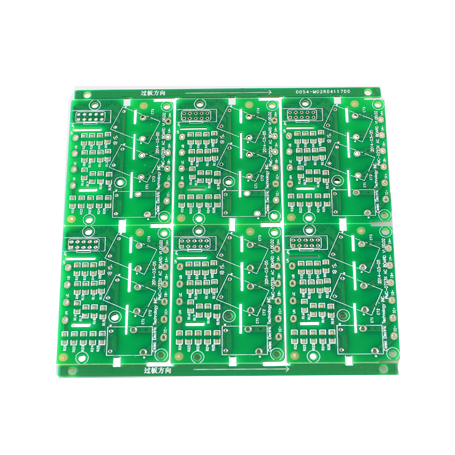
Printed circuit boards (PCBs) are essential components in most electronic devices and products. They provide the foundation on which chips, resistors, capacitors and other components are mounted and connected. As products become more complex and miniaturized, the demands on PCBs increase. Manufacturers need PCBs that are high density, reliable and cost effective. This article explores how its possible to get cheap PCB manufacturing and assembly without sacrificing quality.
One of the best options for low cost, high quality PCBs is HILLMANCURTIS PCB. This company based in China offers full turnkey services for PCB manufacturing and assembly. Here are some of the key benefits HILLMANCURTIS provides: Assembly And Fabrication
HILLMANCURTIS leverages its scale, vertical integration and location in China to offer very competitive pricing. For medium to high volume orders, prices can be 60-70% lower than US based manufacturers. Even for prototypes, their pricing is very reasonable.
Despite the low costs, HILLMANCURTIS does not compromise on quality. They use the latest equipment and processes to manufacture PCBs to IPC Class 2 and 3 standards. Rigorous testing ensures reliability and functionality.
Standard production time is just 3-5 days for simple PCBs and 7-15 days for complex designs. Faster turnaround is available for an additional fee. Their streamlined online ordering and DFM checks speed up the process.
HILLMANCURTIS offers discounted pricing for PCB prototyping. This allows validation of design concepts before investing in full production. They also provide advanced services like PCB routing and layout.
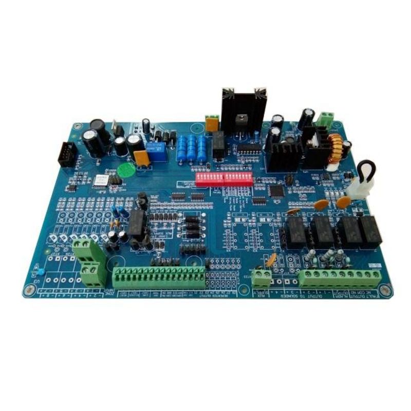
In addition to bare PCB manufacturing, HILLMANCURTIS provides complete assembly of components on the PCBs. This includes soldering of SMT and through-hole parts. They have capability for high density components and fine pitch soldering.
Their website provides complete information and instant pricing quotes. The sales team provides guidance on DFM, testing and other technical matters. Production status is visible online and quality issues are resolved quickly.
With its combination of affordable pricing, quality manufacturing, rapid turnaround and assembly services, HILLMANCURTIS PCB is an excellent choice for electronics companies. Their one-stop solution reduces hassles and enables faster time to market.
To leverage the benefits of low cost PCB production and assembly, the PCB design needs to follow certain guidelines. This facilitates manufacturing and improves yields. Here are some key considerations:
Optimal panel utilization occurs when board dimensions correspond to standard PCB panel sizes like 200mm x 300mm or 300mm x 400mm. Non-standard sizes cost more.
Higher layer counts add complexity and increase costs. Aim for 2-8 layers unless more are essential for routing density.
Standard component packages are easier to source and assemble. Avoid odd shaped parts and connectors. Follow industry standard footprints.
Use minimum trace widths and spacings for the target PCB class. This maximizes routing density. Allow adequate isolation for high speed signals.
Provide sufficient annular rings (clearance) around pads for reliable solder joint formation. Recommended values are 0.2mm to 0.3mm annular ring.
Place reference designators, polarity markings, component values and other silkscreen labels appropriately to aid assembly. Allow clearance from pads.
Include adequate test points to validate functionality, especially for prototyping. Test points can be removed later to reduce costs.
By designing PCB layouts that follow these guidelines, cheap PCB fabrication and assembly can be realized without compromising quality and reliability.
Understanding the PCB manufacturing process helps identify potential issues early so they can be addressed in the design phase. Here are the key steps:
The PCB layout is designed in CAD software like Altium, KiCad, Eagle etc. The Gerber files are generated which provide the artwork mask data.
The PCB manufacturer reviews the design to ensure manufacturability. Feedback may be provided requesting changes.
For volume production, multiple PCBs are arranged on larger panels to maximize material utilization.
Sheets of copper clad laminate are stacked and glued together under heat and pressure to create a multilayer board.
High speed CNC drilling machines create all the holes needed for vias and component leads.
The walls of drilled holes are plated with copper to form the interconnects between layers.
The desired circuit pattern is transferred onto each copper layer using an image transfer and etching process.
Chemicals dissolve away unwanted copper leaving only the copper traces and pads.
A lacquer layer is applied to protect copper traces from oxidation and prevent solder bridges.
Markings like reference designators and symbols are printed to identify components.
Individual PCBs are cut apart from the larger panels if required.
Electrical tests validate connectivity and pinouts. Automated optical inspection ensures quality.
For full turnkey PCBs, components are soldered onto the boards before final testing.
While bare PCB fabrication is inexpensive, companies often still need to hand assemble and solder components. By opting for full turnkey PCB assembly, additional benefits can be realized:
Many leading PCB manufacturers offer assembly services spanning the full spectrum from prototyping to high volume production. With stringent quality control and process capability, the assembled boards function identically to in-house assembly. Hence leveraging turnkey assembly enables companies to shorten product launch cycles at lower risk and cost.
A: The main factors that impact cost are board size, layer count, quantity, lead time, material (FR4, Rogers, ceramic etc.), trace/space, hole size/quantity, finishes, tolerances, and special processes like impedance control or HDI.
A: Most PCB manufacturers like HILLMANCURTIS provide an online quoting tool where you can enter details about layers, size, quantity, finishes etc and get an immediate quote. Uploading Gerber files gives the most accurate pricing.
A: For standard 2-8 layer designs in medium volumes, the lead time is usually 3-5 days for prototype small batches and 7-15 days for larger production orders. For complex PCBs or large orders, lead times can extend to 4-6 weeks.
A: Yes, their engineering team can review designs before ordering and provide feedback on DFM, stackup, layer count, etc to ensure manufacturability. They also offer layout services if needed.
A: A pick and place assembly file (CSV or XLS usually) indicates the component types, quantities, positions and rotations. This generates the machine programming for automated assembly.
Use Of Pcb Board © 2023 Benzinga.com. Benzinga does not provide investment advice. All rights reserved.